
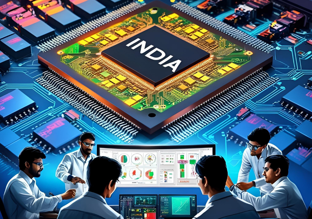
In a historic leap forward, the India semiconductor industry has officially entered the 3-nanometer (3nm) chip design era, marking a significant moment in India’s journey towards becoming a global semiconductor powerhouse. Union Electronics and IT Minister Ashwini Vaishnaw inaugurated two new Renesas Electronics design centres in Noida and Bengaluru, ushering in a new age of advanced semiconductor innovation.
“This is a next-generation leap. We’ve done 7nm and 5nm earlier, but designing at 3nm is truly a frontier,” said the Minister, celebrating India’s transition into cutting-edge chip design.
India Joins the Global 3nm Club
Designing chips at the 3nm scale is considered a hallmark of semiconductor innovation, given its enhanced performance, lower power consumption, and complexity. India’s inclusion at this level signifies not just technological progress but also international credibility.
Speaking at the event, Ashwini Vaishnaw said:
“In a first, 3nm chips will be designed in India.”
This announcement places India in an elite group of nations working on ultra-small node semiconductors, currently dominated by countries like Taiwan, South Korea, Japan, and the United States.
Strategic Centres in Noida and Bengaluru
The new Renesas Electronics India Private Limited centres are expected to drive:
- Next-generation chip design for AI, IoT, mobility, and consumer electronics
- Collaborations with global supply chains in fabrication and assembly
- Innovation in embedded systems and edge computing
The Noida centre will strengthen India’s electronics innovation in the north, while the Bengaluru hub will tap into deep tech talent and the city’s existing semiconductor ecosystem.
🔗 Also Read: Operation Sindoor: How India Responded to Pahalgam Terror Attack »
India Semiconductor Industry: Vision and Roadmap
Minister Vaishnaw outlined India’s comprehensive semiconductor vision, encompassing:
- Chip design
- Fabrication (foundries)
- ATMP – Assembly, Testing, Marking, Packaging
- Support infrastructure – equipment, chemicals, gas, tools
- Skilled manpower development
He noted that the India Semiconductor Mission (ISM) is already facilitating partnerships and investments from global players like Applied Materials and Lam Research, with positive signals at global forums like Davos.
Semiconductor Learning Kits for Students
In another key announcement, Vaishnaw launched a Semiconductor Learning Kit that will be distributed across 270+ academic institutions that already use advanced EDA tools under the ISM.
Key Benefits:
- Hands-on hardware exposure for engineering students
- Integration of design software and embedded systems
- Creation of industry-ready talent pool
“This is not just infrastructure—it’s long-term investment in talent,” the minister said.
The learning kits will serve as a foundation for building India’s next generation of semiconductor engineers, essential for sustaining momentum in the India semiconductor industry.
Why 3nm Design Matters
Chips at 3nm offer:
- Faster performance at lower power consumption
- Greater transistor density, enabling powerful computing in smaller form factors
- Application across smartphones, servers, medical tech, defense, and autonomous vehicles
With global demand for semiconductors skyrocketing, especially in AI and connected devices, India’s foray into 3nm design positions it strategically in future-ready manufacturing.
Renesas: Strategic Partnership With India
Hidetoshi Shibata, CEO and MD of Renesas Electronics, called India a “strategic cornerstone” for their global roadmap.
“India’s embedded system talent and strategic alignment with Japan will reshape the global semiconductor landscape,” he said.
Renesas has already collaborated with Indian startups, research labs, and automotive players, particularly in embedded systems and low-power applications. This expansion into 3nm R&D is expected to accelerate India’s deep-tech growth.
🔗 Also Read: India Reaffirms Demand for Return of Pakistan-Occupied Kashmir»
Government Push for Self-Reliance in Semiconductors
The Indian government is aggressively promoting semiconductor self-reliance through:
- ₹76,000 crore incentive package for semiconductor manufacturing
- Approval of multiple chip fabrication plants
- Streamlined policies on electronics design clusters (EDCs)
- MoUs with Japan, the US, and Taiwan for R&D cooperation
The IT ministry’s latest move signals that design leadership is just as important as domestic fabrication. Design-led manufacturing will reduce India’s dependency on imports and improve its position in the global value chain.
Global Demand and India’s Timely Entry
Global semiconductor demand is expected to double by 2030, driven by:
- 5G and AI expansion
- Smart vehicles and mobility solutions
- Healthcare and robotics integration
- Cybersecurity and military applications
India’s 3nm capability positions it as a serious contender in attracting global business for chip IP design and allied sectors.
Conclusion
The launch of 3nm chip design in India is more than just a technological achievement—it’s a symbol of intent. With the government’s unwavering support, rising private investments, and a robust talent pool, the India semiconductor industry is now stepping confidently onto the global stage.
Ashwini Vaishnaw’s announcement underscores a strategic shift from being a consumer of technology to a creator, marking the beginning of a new era in India’s tech sovereignty.